
Нарезка на кубики - важный этап производства полупроводников, на котором производители разрезают кремниевые пластины на отдельные чипы или матрицы. Традиционно в этом процессе используются пильные диски или лазеры, которые прорезают пластину вдоль канала для нарезки, отделяя чипы и подготавливая их к упаковке и установке в готовые устройства. Однако постепенно набирает популярность плазменная обработка, в которой используется фторсодержащая плазма для сухого травления, чтобы удалить материал из канала для нарезки. Поскольку микросхемы продолжают уменьшаться в размерах и становятся все меньше, тоньше и сложнее, плазменная обработка все чаще рассматривается как предпочтительный выбор в отрасли благодаря своим неоспоримым преимуществам.
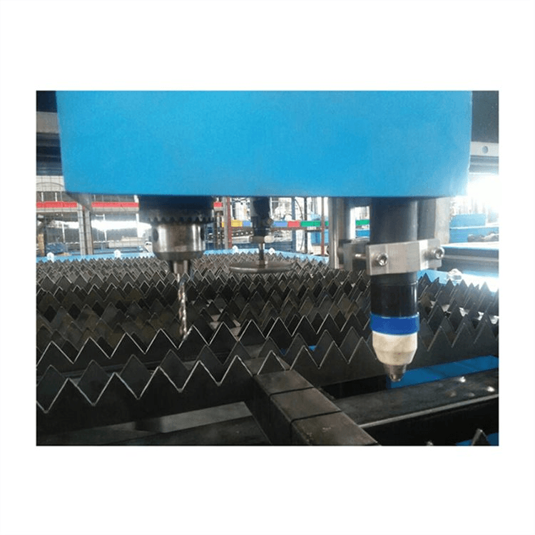
Нарезка лезвиями
При лезвийной обработке используется высокоскоростное вращающееся абразивное лезвие для прорезания канала между стружками. Как правило, лезвие изготавливается из абразивных материалов, таких как песок или алмазы. Хотя лезвийная обработка эффективна, она основана на механическом удалении материала, что может привести к сколам, трещинам и другим повреждениям штампа. Это часто приводит к снижению выхода продукции и увеличению затрат из-за производства бракованных изделий. Плазменная обработка позволяет избежать этих проблем, предлагая более надежное решение для хрупких микросхем и более высокую общую производительность.
Лазерная резка
Лазерная нарезка кубиками использует сфокусированную лазерную технологию для разрезания пластины. Лазер генерирует высокую концентрацию фотонов, которые нагревают материал до чрезвычайно высоких температур. Под действием интенсивного тепла канал разреза испаряется или аблатируется. В более продвинутых методах, таких как “невидимая лазерная резка”, тепло создает перфорацию в пластине, что в конечном итоге приводит к ее разрушению вдоль канала разреза. Хотя лазерная резка эффективна, она дороже, чем лезвийная, и все равно создает тепловое напряжение, которое может привести к повреждению. Поэтому плазменная резка стала привлекательной альтернативой, преодолевающей эти недостатки.
Преимущества плазменной резки
Повышенная урожайность
Плазменная нарезка предлагает значительные преимущества с точки зрения производительности. Поскольку плазма химически вытравливает материал в канале, не вызывая механических повреждений или зон термического воздействия, она позволяет избежать проблем, связанных с лезвийными и лазерными методами. Это обеспечивает более высокую механическую целостность матрицы, особенно в приложениях с высокими физическими нагрузками, таких как системы памяти с высокой пропускной способностью (HBM). Кроме того, плазменная нарезка кубиков обеспечивает их большую прочность на излом, что снижает вероятность выхода из строя устройств и повышает общую производительность.
Увеличенная пропускная способность
Еще одним ключевым преимуществом плазменной резки является ее способность увеличивать производительность. В отличие от лезвийной и лазерной обработки, которые являются последовательными процессами, позволяющими вырезать по одному штампу за раз, плазменная обработка работает параллельно. Это позволяет одновременно удалять несколько полос напыления. Поскольку размеры матриц продолжают уменьшаться, а толщина пластин уменьшается, плазменная обработка становится все быстрее и эффективнее, предлагая производителям возможность обрабатывать больше пластин за меньшее время. Эта возможность становится особенно важной по мере роста спроса на более компактные и сложные микросхемы.
Больше матриц на пластину
Плазменная обработка позволяет производителям извлекать больше матриц из каждой пластины. В отличие от лезвийной или лазерной обработки, которые ограничены шириной лезвия или размером лазерного пятна, плазма позволяет создавать более узкие каналы для обработки. Это позволяет использовать пластину более эффективно, максимизируя количество активных матриц, которые можно получить. Это особенно важно, поскольку полупроводниковые устройства продолжают уменьшаться в размерах. Возможность увеличить количество матриц на пластине снижает общие производственные затраты и повышает рентабельность.
Гибкость конструкции
Еще одно преимущество плазменной резки - гибкость конструкции. В отличие от лезвийной и лазерной резки, которые требуют прямых траекторий резания, плазменная резка позволяет создавать микросхемы различных форм и размеров. Разработчики также могут удалять защитные кольца и лучше располагать тестовые группы микросхем для оптимизации использования площади подложки. Такая гибкость делает плазменную нарезку идеальной для сложных компоновок микросхем, особенно в передовых полупроводниковых приложениях. Она также дает производителям возможность удовлетворить более специализированные требования к дизайну.
Идеально подходит для хрупких устройств
Плазменное напыление особенно полезно для хрупких устройств, таких как микроэлектромеханические системы (MEMS). Эти устройства, содержащие крошечные подвижные структуры, такие как инерционные датчики, чувствительны к механическим нагрузкам. Немеханическая природа плазменной обработки помогает сохранить целостность этих хрупких компонентов, предотвращая вибрации или физические повреждения, которые могут повлиять на работу устройства. Кроме того, при плазменной нарезке не образуется мусора, что гарантирует отсутствие помех для движения компонентов МЭМС.
Устраняет загрязнение частицами
Еще одним важным преимуществом плазменной обработки является ее способность устранять загрязнение частицами. В отличие от механических методов обработки, которые могут оставлять на поверхности пластин обломки или частицы, при плазменной обработке образуются только газообразные побочные продукты. Эти побочные продукты быстро удаляются с помощью вакуумной откачки, оставляя чистую поверхность пластины. Это очень важно для таких применений, как гибридное склеивание, где загрязнения могут привести к дефектам. Плазменная обработка помогает обеспечить чистоту поверхности пластин, что приводит к созданию более качественных и надежных полупроводниковых устройств.
Будущее полупроводниковой керамики
По мере развития полупроводниковой промышленности и усложнения конструкций микросхем плазменная нарезка выделяется среди других методов нарезки пластин. По сравнению с традиционными методами, такими как лезвийная и лазерная резка, плазменная нарезка предлагает повышенную производительность, более высокую механическую целостность и более высокую пропускную способность. Способность создавать более узкие каналы для нарезки кубиками также позволяет увеличить количество кубиков на пластину, что максимально повышает эффективность использования пластин. Кроме того, гибкость плазменной резки позволяет создавать сложные конструкции и особенно хорошо подходит для хрупких устройств, таких как МЭМС. Благодаря этим значительным преимуществам плазменная обработка может играть все более важную роль в производстве полупроводников, повышая эффективность и снижая совокупную стоимость владения.


